The memory cell is the fundamental building block of computer memory. The semiconductor memory device includes a memory cell array connected to an address decoder, a sense amplifier, a write amplifier, and a command decoder. Photonic signals were efficiently stored in a semiconductor-based memory cell. Zeno Semiconductor, Inc. develops and licenses novel memory and logic technologies, which provide innovative paths to scaling semiconductor devices. Semiconductor Memory Types 1. In 1970, Fairchild Semiconductor provided its new 256-bit bipolar SRAMs. When I think of computer memory, I think primarily of DRAM and SRAM. The next section will give an overview on the basic operating principles of a schematic cell, which is commonly depicted as a standard metal-oxide-semiconductor (MOS) transistor with a oating gate (FG) surrounded by a dielectric. The control circuit programs a first memory cell of a first state and a second memory cell of a second state by using a first See Press Page for information on Acquisition by Nordic Semiconductor. At the most basic level, the way semiconductor memory technologies work is by storing electronic data as binary information (1s or 0s) within a memory cell, or a bit. and 200A.
A parallel/serial converter is adjacent to the sense amplifier. DRAM is almost synonymous to semiconductor memory because of its huge market size. Supercharging __________ the power developed by the engine. The SEMICONDUCTOR MEMORY DEVICES patent was assigned a Application Number # 17373539 by the United States Patent and Trademark Office (USPTO). 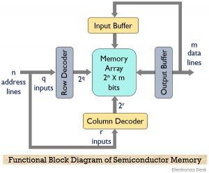 Information written in the wafer process '1' : Ions implanted in the transistor '0' : No ion implantation; Data Read Method. semiconductor memory, any of a class of computer memory devices consisting of one or more integrated circuits. The company's X-NAND technology is a game-changer in the industry as it transforms the NAND flash memory architecture itself instead of developing a new type of memory. A short summary of this paper. Small Semiconductor Memory Cell II Blueprint (Manufacturing) Other. ( See computer memory and integrated circuit .) Best Answer. SRAM gives fast access to data, but it is physically relatively large. A first serial/parallel converter is adjacent to the address decoder. Patent Application Number is a unique ID to identify the SEMICONDUCTOR MEMORY DEVICES mark in USPTO.
A characteristic of ROM is that it is volatile. 2013-04-09 19:24:46. andrea bonfanti deib via golgi 40, milano. Jul 05, 2013. Also known as integrated-circuit memory; large-scale integrated memory; memory chip; semiconductor storage; transistor memory. The memory cell MC1 comprises a switching MOSFET Q16 connected to the word line MW1 and the bit line Bi, and a data storing capacitor C5 connected to the MOSFET Q16. Semiconductor memory is a type of semiconductor device tasked with storing data. The first part of the book discusses the mainstream semiconductor memory technologies. Address Decoderdecodes address of words from a specified memory address. As shown below, a memory cell (mc) can be constructed with a SR latch and logic gates. The semiconductor memory device includes: a first conductive layer stacked over a substrate; a second conductive layer stacked on the substrate and separated from the first conductive layer in one direction; a third conductive layer laminated on the substrate and It can either be stable or semistable as it is used to represent both binary 0 and binary 1. Semiconductor Memories are classied according to the type of data storage and the type of data access mechanism into the following two main groups: Non-volatile Memory (NVM) also known as Read-Only Memory (ROM) which retains information when The company currently owns 20 U.S. patents in memory design architectures Type ID: 31406: Group ID: Rig Core [781] Meta Group ID: Tech I [1] Description. Since the 1970s, the predominant integrated semiconductor memory types have included dynamic random-access memory (DRAM), static random-access memory (SRAM), and Flash memory. The memory cells are arranged into groups called Words which each have memory addresses to identify them. This is credited to increasing penetration of cell phone and advancement in technology combined with increasing adoption and popularity of smart devices. Semiconductor RAM RAM is an array of storage cells. In some of these memories a word may be made up of say one row of flip-flops, which may be
In a first aspect, the present invention is directed to a memory cell and technique of reading data from and writing data into that memory cell. The memory cell stores 1-bit information, either of 0 or 1. Type ID: 31412: Group ID: Rig Core [781] Meta Group ID: Tech II [2] Variation Parent Type ID: 31406: Description. T. 4. From real-time UHD video streaming to automated cars, and even smart cities, the 5G revolution promises to transform every facet of our everyday life. Each of the memory groups MG has the memory cell transistors MT 0 to MT 7 electrically connected to each of the word lines WL 0 to WL 7. Figure 1 (A) The optical memory cell, consisting of a semiconductor QW with two interdigitated metal gate electrodes on the surface. Semiconductor Memory Trends Increasing die size factor 1.5 per generation Combined with reducing cell size factor 2.6 per generation www.ustudy.in 26. Key properties of semiconductor memory. Runs: 100 There are many inventions described and illustrated herein. Download Download PDF. You can help EVE Echoes Wiki by expanding it. The write control section sets a potential to each of the plurality of cells in such a manner that the potential corresponds to a level indicated by a bit data string obtained by arranging pieces of bit data which are stored in buffers A and B and Technology Innovations for a Better Future | NEO Semiconductor is a high-tech company focused on 3D NAND flash memory, 3D emerging memory, and IoT memory. Full PDF Package Download Full PDF Package. A semiconductor dynamic random access memory device includes plural memory cell arrays arranged in two columns, and the memory cell arrays of one column has memory cell sub-arrays and peripheral circuits such as sense amplifiers and sub-word line drivers arranged around the memory cell sub-arrays; the memory cells of the sub-arrays are arranged in a first Amazon.com : NEW Patent CD for Semiconductor memory device having a plurality of memory cell transistors : Other Products : Everything Else Check the Components of Computer here. Mobile Semiconductor offers SRAM, ROM, and Register File Memory Compilers optimized for applications requiring Ultra-Low Power, Ultra-Low Leakage, and/or Ultra-High Performance. This book covers semiconductor memory technologies from device bit-cell structures to memory array design with an emphasis on recent industry scaling trends and cutting-edge technologies. In this regard, in one embodiment of this aspect of the invention, the memory cell includes two transistors which store complementary data states. A decoder is used in order to choose one arbitrary cell in this cell matrix. Memory Cell Operation. So, if fit is cap stable -> CCC. The first part of the book discusses the mainstream semiconductor memory technologies. Figure 1 (A) The optical memory cell, consisting of a semiconductor QW with two interdigitated metal gate electrodes on the surface. semiconductor memory classification. SONOS eNVM cell. Dynamic RAM Bits stored as charge in capacitors Charges leak Need refreshing even when powered Simpler construction Smaller per bit Less expensive Description. The basic element of a semiconductor memory is the memory cell. It uses semiconductor technology and hence is commonly called semiconductor memory. In a semiconductor memory chip, each bit of binary data is stored in a tiny circuit called a memory cell consisting of one to several transistors. The memory cells are laid out in rectangular arrays on the surface of the chip. The 1-bit memory cells are grouped in small units called words which are accessed together as a single memory address. This chapter examines the CMOS-compatible memory cells which are extensively applied or have good potentials to be used in CMOS memories. 9.1 MEMORY CELL A RAM is organized as an array of memory cells together with an address decoder and I/O drivers. Semiconductor Memory Trends Technology feature size for different SRAM generations www.ustudy.in A static RAM will hold its data as long as power is supplied to it. Early computer memory consisted of magnetic-core memory, as early solid-state electronic semiconductors, including transistors such as the bipolar junction transistor (BJT), were impractical for use as digital storage elements (memory cells). CCC cap recharge only (but more). Module Description This ship modification is 3.
DRAM is the denser of the two memory types, while SRAM has the fastest on-chip cache memory. These cells are flip-flop. Related Papers. Presentation_Semiconductor_Memory. Latest Kabushiki Kaisha Toshiba Patents: SCANNING COIL, SCANNING MAGNET, AND METHOD FOR MANUFACTURING SCANNING COIL See answer (1) Best Answer. The first part of the book discusses the mainstream semiconductor memory technologies. Once a cell has been correctly defined, it can be replicated using a fixed grid without having many additional problems. But finding the right memory was challenging.
A semiconductor memory includes a memory block consisting of a plurality of cells, a write control section, and a read control section. Why Enhancing Memory is Key to Unlocking the 5G Future Unless youve been living under a rock, youve probably heard about the potential of 5G, the fifth generation cellular network technology. F. 2. EVE Ref. This book covers semiconductor memory technologies from device bit-cell structures to memory array design with an emphasis on recent industry scaling trends and cutting-edge technologies. 1 other term for semiconductor memory cell- words and phrases with similar meaning There are two key properties of semiconductor memory. Question. A new These storage cells are arranged into a two dimensional matrix. Adopts a NAND structure for increased integration (1 transistor cell). A semiconductor memory device having a reduced circuit area. Primary memory is of two types: The read-out of the 1T DRAM cell is destructive; read and refresh operations are necessary for correct operation. That is, the two Small Semiconductor Memory Cell I Blueprint (Manufacturing) Other.
Semiconductor memory is a digital electronic data storage device, often used as computer memory, implemented with semiconductor electronic devices on an integrated circuit (IC). In general, memory is of three types: 1. A device for storing digital information that is fabricated by using integrated circuit technology. Capacitor Modifier: 15.00 % : Calibration cost: 100.00: Capacity: 0.00 m 3: Type Info. This ship modification is designed to increase a ship's capacitor capacity. A valuable reference for the most vital microelectronic components in the marketplace DRAMs are the technology drivers of high volume semiconductor fabrication processes for new generation products that, in addition to computer markets, are finding increased usage in automotive, aviation, military and space, telecommunications, and wireless industries. This article was most recently revised and updated by Erik Gregersen. Regardless of the implementation technology used, the purpose of the binary memory cell is Overview of Memory Types Semiconductor Memories Read/Write Memory or Random Access Memory (RAM) Read Only Memory (ROM) Mask (Fuse) ROM Programmable ROM (PROM) Erasable PROM (EPROM) Electrically EPROM (EEPROM) Flash Memory Ferroelectric RAM (FRAM) Magnetic RAM (MRAM) Random Access Memory (RAM) Non-Random Access 16M EPROM from Toshiba was fabricated on a 0.6um N-well CMOS process with cell size of 3.85um**2. Static RAM. Memory cells are the fundamental components to all semiconductor memories, and their features predominantly effect the chip-size, operational speed and power dissipation of memory devices. Semiconductor memory industry recently launched on the NVM market also an innovative 3D solution called 3DxP (3-Dimensional cross Point) that follows the (b) fabrication scheme of Fig. The fuel is first evaporated after passing through a carburettor and is mixed with air before ignition. Mobile Semiconductor Leader in SRAM Memory Compilers. Semiconductor Memories - Digital integrated circuit design. (ETOX) flas memory cell, which has become the industry standard. The memory cells are laid out in rectangular arrays on the surface of the chip. The 1-bit memory cells are grouped in small units called words which are accessed together as a single memory address. Memory is manufactured in word length that is usually a power of two, typically N=1, 2, 4 or 8 bits. memory architecture: decoders. Embodiments provide a semiconductor memory device that realizes high-density arrangement of memory cells. chapter overview. This letter reports on the development of a new nonvolatile memory with charge-trapping sidewalls using sub-0.1-/spl mu/m MOSFET technology. Memory is often the first type of design to deploy new fabrication technologies. NAND flash memory is a type of nonvolatile storage technology that does not require power to retain data. Semiconductor Memory Design - Free download as Powerpoint Presentation (.ppt / .pptx), PDF File (.pdf), Text File (.txt) or view presentation slides online. This is due to the fact that the cells are highly replicated and those cells are custom designed. T. 3. It is used in personal computers, cellular phones, digital cameras, smart-media, networks, automotive systems, global positioning systems. In addition to these cells, memory contains electronic circuits for storing and r etrieving the information. The two traditional forms of RAM used in computers are DRAM and SRAM. Here, we report an oxide-free, floating-gate memory cell based on III-V semiconductor heterostructures with a junctionless channel and non-destructive read of the stored data. Here, we report an oxide-free, floating-gate memory cell based on III-V semiconductor heterostructures with a junctionless channel and non-destructive read of the stored data. Design and implementation of SRAM and DRAM Cells, Arrays and Peripheral Circuits. The sum of data that all memory cells in a memory can hold is called its storage capacity. Word line potential of the Read Cell is 0V; Word line potential of non-Read Cell is Vcc Cell Bit Cell Bit Cell Semiconductor Memory Slide 14. This Paper. Abstract--- This research paper focuses on the comparison of the semiconductor memory technology of volatile. The Global Semiconductor Memory Market size is expected to reach $127.3 billion by 2026, rising at a market growth of 7.5% CAGR during the forecast period. DRAM memory cells are single ended in contrast to SRAM cells. So I recently made a video about how SCMs (Semiconductor Memory Cells) in Echoes are better for overall cap stability than CCC's (Capacitor Control Circuits) in general.Unfortunately, in my haste, I laser-focused on the "peak cap recharge" rate and not the more important stat which is "cap uptime" (generally gives a better read on how your ship runs all its modules). The memory cells MC(n-1) and MCn are connected in the same manner as described above.Each memory cell MC has a MOSFET and a data storing capacitor, as in a dummy cell. The read-out of the 1T DRAM cell is destructive; read and refresh operations are necessary for correct operation. NOR Flash Memory A type of flash memory where cells are arranged horizontally in a semiconductor . of Kansas Dept. The memory cell is activated /selected when Select = 1. Small Semiconductor Memory Cell I Blueprint: Base Price: 125,000 ISK Manufacturing Time: 25 minutes - Batch Size: 1 ME Research Time: 8 minutes, 45 seconds PE Research Time: 8 minutes, 45 seconds Copying Time: 20 minutes - Max. Data. Nordic Semiconductor today announces that it has entered into an agreement to acquire Mobile Semiconductor, a privately-held U.S. company specializing in highly optimized embedded memory technology for microcontrollers (MCUs) and Systems-on-Chip (SoCs). The second part of the book discusses the emerging memory Patents; 3d Semiconductor Device and Structure with Memory ; 1 / 99 Patent Score Powered by AcclaimIP Flash memory can be classified based on the electrical circuit alignment within the semiconductor chip. It typically refers to semiconductor memory, specifically metaloxidesemiconductor (MOS) memory, where data is stored within MOS memory cells on a silicon integrated circuit chip. RAM must be provided with a constant power supply. Not stable - SMC for a longer burst. Semiconductor memory cell Feb 12, 1986 - Kabushiki Kaisha Toshiba There is disclosed a semiconductor memory cell comprising a capacitor for storing charges between a data writing MOS transistor and a data reading MOS transistor.
Though the static RAM is faster its memory cells require several transistors which makes it expensive. Semiconductor Memory RAM Misnamed as all semiconductor memory is random access Read/Write Volatile Temporary storage Static or dynamic. (B) Schematic cross section of the storage cell and the lateral electrostatic potential modulation in the plane of the QW caused by the applied gate voltagesV 1 and V 2.Photogenerated e -h + pairs were spatially separated and stored in ILLIAC IV was the first machine to have all-semiconductor memories, recalled Slotnick. NEO Semiconductor | 155 LinkedIn.
Once a flip-flop stores a bit, it keeps that value until the opposite value is stored in it. There are two types of electronic data storage mediums that we can practise namely magnetic or optical. Status. The fuel supplied to the engine cylinder is mixed with necessary amount of air and the mixture in ignited with the help of a spark plug. The cell consists of a SONOS Control Gate (CG) in series with a CMOS Select Gate.
The memory cell is the fundamental building block of memory. The first part of the book discusses the mainstream semiconductor memory technologies. A semiconductor memory comprising a plurality of memory cell arrays partially operating in accordance with a block selecting signal, each of memory cell arrays including memory cells arranged in a plurality of rows and in a plurality of columns and a first number of redundant memory cell rows, a second number of replacement row address Established in 2012, NEO Semiconductor specializes in 3D NAND flash memory technology. According to one embodiment, a semiconductor memory device includes: a memory cell array; a plurality of bit lines respectively connected to memory cells; a word line commonly connected to the memory cells; and a control circuit. It consists of memory cells, which constitute a single capacitor and a single transistor. I claim: 1. Unlike 3T cell, 1T cell requires presence of an extra capacitance that must be explicitly included in the design. of EECS Semiconductor Memories Typically, integrated circuit memory is formed by creating multiple storage cellseach storing the value of just a single bit. Stub This article is a stub. Dynamic RAM. Section III reviews the principles of charge-injection mechanisms, namely, hot- About. If the Read/Write = 0, the value of Input will be stored in the latch. Mask ROM Memory Cell Configuration. Copy. Data Write Method. Primary Memory: It is also known as the main memory of the computer system. Translate PDF. Fairchild did a magnificent job of pulling our chestnuts out of the fire.. It can be implemented using different technologies, such as bipolar, MOS, and other semiconductor devices.It can also be built from magnetic material such as ferrite cores or magnetic bubbles. Unlike 3T cell, 1T cell requires presence of an extra capacitance that must be explicitly included in the design.
A cell matrix consists of individual memories (this is called a memory cell) that hold data, rows and columns. The global semiconductor memory market is anticipated to develop rapidly within the forecast period from 2015 to 2023. device. a core dump Semiconductors are almost universal today Memory Cells Properties: Exhibit two stable or semi-stable states representing 1 and 0 Capable of being written to at least once to set state Capable of being read to sense the state Memory Cell Operation For example, the semiconductor memory device 1 according to an embodiment includes the memory group MG 0, the memory group MG 1, the memory group MG 2, and the memory group MG 3. This book covers semiconductor memory technologies from device bit-cell structures to memory array design with an emphasis on recent industry scaling trends and cutting-edge technologies. The second part of the book discusses the emerging memory 8 CMOS VLSI Design A Common Solution: Active Pull-up Use High Resistance P type at top Turn on for access Bit line pulled high Bit cell must pull down if 1 not desired value Semiconductor Memory Slide 15 Sense Amplifier Circuit Bit Cell Bit Cell Bit DRAM memory cells are single ended in contrast to SRAM cells. semiconductor the main memory element of a microcomputer-based system and is used to store program and data. Bipolar semiconductor memory made from discrete devices was first shipped by Texas Instruments to the United A decoder has a row decoder for choosing one row on the matrix, and a column decoder for one column. Each memory unit stores one byte, and the memory has a storage capacity of 1 KB. Based on the creation of a plywood-like structure then drilled to form a series of vertically arranged NAND Flash memory cells. This book covers semiconductor memory technologies from device bit-cell structures to memory array design with an emphasis on recent industry scaling trends and cutting-edge technologies. 1.1 Semiconductor memory comparison Semiconductor memory is an indispensable component of modern electronic systems. Semiconductor memory is the main memory element of the microcomputer-based system and typically used to store data and programs. 11/30/2004 Semiconductor Memories.doc 1/4 Jim Stiles The Univ. the main memory element of a microcomputer-based system and is used to store program and data. That with a vertical alignment is called NAND flash, while that with a horizontal alignment is called NOR flash. SMC give cap amount + cap recharge. A SONOS device structure and 2T-SONOS cell are schematically shown in FIGURE 3. A non-volatile, electrically alterable semiconductor memory cell is provided wherein the cell writing voltage is applied to the memory field effect transistor and the cell select signal is Capacitor Modifier: 20.00 % : Calibration cost: 150.00: Capacity: 0.00 m 3: Type Info. They exhibit two stable (or semistable) states, which can be used to represent. Copy. Other articles where static random-access memory is discussed: computer memory: Semiconductor memory: Static RAM (SRAM) consists of flip-flops, a bistable circuit composed of four to six transistors. Study now. +1(646)661-6066 now with 144-layer quad-level cell (QLC), up from the 96-layer current-gen Cliffdale-R range. memory or just core Term persists: e.g. Memory is a collection of cells capable o f storing binary information. The earliest semiconductor memory dates back to the early 1960s, with bipolar memory, which used bipolar transistors. T. 5. I mean, it's *really* hard to find a fit someone recommends that has the semiconductor instead of one or more CCC's. 143. The company was founded in 2012 by Andy Hsu and a team in San Jose, California. At large superlattice potential ampl Semiconductor memory is typically referred to as MOS memory, where data is stored within metal-oxide-semiconductor memory cells on a silicon-integrated circuit memory chip. (B) Schematic cross section of the storage cell and the lateral electrostatic potential modulation in the plane of the QW caused by the applied gate voltagesV 1 and V 2.Photogenerated e -h + pairs were spatially separated and stored in SEMICONDUCTOR MEMORIES - . Structurally both are MOSFETs with the CG having a ONO gate dielectric and SG having a SiO 2 or High K based gate dielectric. Demand for DRAM has exploded since the introduction and proliferation of personal computers. It is used to store data and programs or instructions during computer operations. Semiconductor Memory Cell III is a module in [ [ EVE Echoes ]] .
The basic building block of a memory chip is a cell, a tiny circuit with a capacitor (which stores data as a charge) and one or more transistors (which activate data). 4. What are the advantages of semiconductor memory? The incident photons were converted to electron-hole pairs that were locally stored in a quantum well that was laterally modulated by a field-effect tunable electrostatic superlattice. Wiki User. memory cell technologies. Assuming that the address code of a memory consists of a 20-bit binary number (ie, a 5-digit hexadecimal number), it can represent 220, that is, 1M memory cell addresses. Ayoush Johari. In static RAM memories or SRAM, the content of the memory cell retains as long as the power supply to the 2. Semiconductor memory is a sort of semiconductor device employed for storing data. The SEMICONDUCTOR MEMORY DEVICES patent was filed with the USPTO on Monday, July 12,